Tiny particles help solve big problems
What if the answers to our most pressing challenges, from clean energy to advanced technology, were hidden in a world too small to see? For Dalaver Anjum, that world is his laboratory.

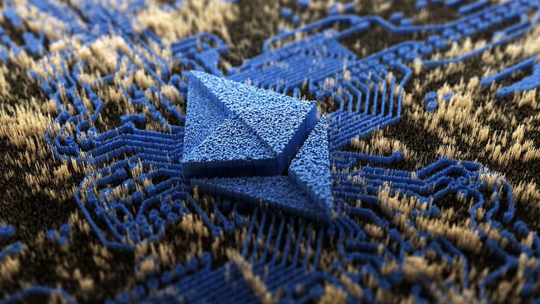
Using powerful transmission electron microscopy (TEM) techniques, Anjum can visualize materials at an atomic level by passing a beam of electrons through them and measuring what comes out the other side. This technique is helping him design solutions for a better and more sustainable future.
How did you discover your passion for transmission electron microscopy?
As part of my PhD studies, I wanted to explore the complex problem of making the tiny, intricate parts inside electronic devices even smaller and better. To do this, I needed to see and understand materials at an incredibly small scale. I tried various characterization techniques, but I was most drawn to electron microscopy which lets you zoom in far beyond what a regular microscope can see. This initial exposure set the course for my career, and I have since used electron microscopy in various environments, including at research institutes, industry and universities.
What’s the most exciting discovery you’ve made so far?
For two decades, I have contributed to advancing both electron microscopy methodology and applications, using them to address a diverse range of challenges in materials. I was the first to successfully analyze liquid mercury with an electron microscope. I also found a way to create a map of a metal’s stiffness at a tiny scale, which helps us understand how strong a material is at its most fundamental level.
“By visualizing and engineering materials at the atomic scale, we can precisely control their structure and properties”.
Dalaver Anjum
In applied research, my work has helped explain the relationship between a material’s atomic structure and its properties. For example, I’ve studied catalysts that can make clean energy by helping to split water into hydrogen and oxygen. I’ve also worked with materials that can help reduce carbon dioxide in the air and others that can turn sunlight into fuel.
What challenges are you tackling now?
My current research addresses the properties of high-strength structural materials and next-generation electronics for wireless communications. My group uses state-of-the-art microscopes and tools that allow us to analyze materials at the atomic level.
All of these represent a significant investment by Khalifa University which provides an exceptional setting for advanced electron microscopy research, offering cutting-edge facilities for atomic-scale imaging and materials characterization.
How might your work change our everyday lives?
My work aims to translate fundamental materials discoveries into technologies with societal benefits. By visualizing and then engineering materials at the atomic scale, we can precisely control their structure and properties. In addition to energy storage and catalysis, this enables the creation of high-performance materials for next-generation aluminum alloys and wireless communications.
These innovations can contribute to sustainable energy systems, cleaner manufacturing, advanced communications beyond 5G, and more efficient transportation. This will help us bridge the gap between laboratory breakthroughs and commercial applications, while supporting global sustainability goals.
What do you hope will be the most significant breakthrough in TEM in the next decade?
In the coming decade, I expect us to be able to create real-time, atomic-scale moving pictures of devices as they work. Imagine watching how a battery charges or how a catalyst reacts, atom by atom, right as it’s happening. This could pave the way for effective tools for real-time condition monitoring of battery energy storage systems that can be utilized to develop advanced control strategies that extend battery lifetime.
Advances in cryogenic four-dimensional STEM, electron ptychography, and low-dose phase-contrast TEM will make it possible to map quantum states—opening up possibilities for quantum computing components and low-energy electronics.
Another transformative frontier will be AI-driven self-driving microscopes that can think for themselves. They’ll be able to acquire, analyze and interpret data, and rapidly screen vast numbers of samples. This will speed up the discovery of new materials and technologies in a way we’ve never seen before.