High-speed computing seen through light-enabled circuitry
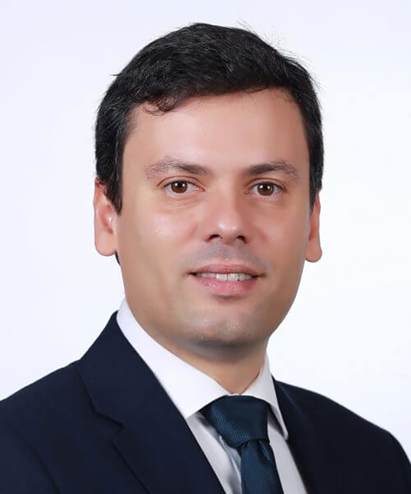
Jaime Viegas, Associate Professor at the Department of Electrical Engineering at Khalifa University.

With seven US patents to his name and a wealth of experience spanning decades, Jaime Viegas delves into the realm of silicon photonics, optical sensors, fiber optic sensors, digital holography, metamaterials design and fabrication. His latest endeavor involves harnessing the power of light-active microelectronics to revolutionize AI algorithm processing.
Can you give us an overview of your research?
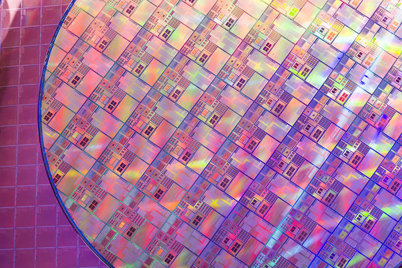
My research mainly focuses on photonics, or light-driven electronics, particularly the development of optical microchips. My team exploits various physical processes integrated in miniaturized systems that fit into a microchip.
We moved from using optical microcircuits for communication and sensing to AI photonic chips. Over the past three years, we have concentrated on implementing AI algorithms using photonic components for high-bandwidth processing. These microchips promise to enhance data-stream processing efficiency, boosting processing speeds while saving energy.
Which key discovery has influenced your current research and how?
Researchers are actively developing new computational paradigms using photonic and quantum computing, driven by the increasing data-gathering and storage capacities of cloud-computing systems. There is a need to further increase computational power while minimizing energy consumption. We are applying our expertise in miniaturizing light circuits to implement specific functions capable of achieving those ultra-highspeed computational steps at chip level.
“Some of our designs are directly incorporated into the market, especially when dealing with miniature modules. Nevertheless, the research journey involves designing and validating, and depending on the foundry’s plans, the products may become part of their technology offerings.”
How did your research journey lead you to your current position at Khalifa University?
I was a PhD student at the University of Porto in Portugal and did my research residency at the University of North Carolina at Charlotte, working on photonic sensors. I spent a year and a half in Charlotte to gain experience in photonic fabrication. Through contacts at MIT, I learned about opportunities at the Masdar Institute, one of three universities that eventually formed Khalifa University. In line with the UAE government’s interest in semiconductors, they were looking for people with experience in photonics and clean-room processing, which led to the Microsystems Engineering program that I joined about 13 years ago, and in which I’ve set up the first photonics lab and cleanroom for microfabrication in the country.
Collaboration is key to research and innovation. Tell us about your ongoing collaborative projects.
Our primary industrial partner is GlobalFoundries, a leading semiconductor chip manufacturer. This collaboration has been crucial in providing our students with early access to cutting-edge semiconductor processes for photonic and radiofrequency microsystems.
We’ve tackled challenges in integrated photonics components, addressing issues where a cascade of devices don’t perform as expected. Traditionally, heaters were used to fix these mismatches but, with collaborators from GlobalFoundries, our students proposed a solution considering the curvature of light during the design phase. This eliminated the need for heaters, improving device performance. The collaboration resulted in several patents for components with enhanced performance, showcasing the practical impact of our work.
What are the major challenges in microsystems engineering?
One significant challenge is finding students willing to learn across diverse disciplines, from electronics and thermal sciences to optics and mechanics. Integration also poses a challenge when combining materials and processes that may be incompatible or lack scalability for real-life applications.


